New compound semiconductor centre for Wales
Compound Semiconductor Applications Catapult centre to drive innovation in multi-billion pound market.
Compound semiconductors such as gallium arsenide (GaAs) and gallium nitride (GaN) are central to development of the 5G network, new high-efficiency LED lighting, power electronics for the next generation of electric vehicles and new imaging techniques for a variety of uses from security to health diagnostics, with the global market for compound semiconductors expected to be £125 billion by 2020.
The centre is backed by wafer maker IQE and Cardiff University who set up the £20m Compound Semiconductor Centre, which will form a key resource to the new Catapult. The partnership will help transform leading edge research at Cardiff University’s new Institute for Compound Semiconductors (ICS) to be built on the University’s new £300m Innovation Campus.
The Catapult for semiconductors will be the 11th Catapult centre. Catapults already exist in:
- cell therapy
- high value manufacturing
- offshore renewable energy
- satellite applications
- digital
- transport systems
- future cities
- energysystems
- precision medicine
- medicine technologies
They are overseen by Innovate UK and join entrepreneurs, engineers and scientists with state-of-the-art facilities that allow them to create new products and services.
Bristol researchers aim for super-bright LEDs
Researchers in Bristol are working on a European project to increase the performance of white LEDs by a factor of 10 for brighter car headlights.
The €3.8m GECCO project aims to use vertical structures for the new LEDs. Modern high-performance LEDs already provide a bright light output at high efficiency and are used for automobile headlights. At present though, the production process for these kinds of LEDs is still not cost efficient enough and also the efficiency of these LEDs needs further improvement.
The international team of the GECCO project includes the Technical University of Braunschweig in Germany, Madrid, Lodz and lighting company OSRAM in Munich and Regensburg.
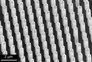
Up to now, LEDs are being constructed in a planar way, meaning in layers and completely flat. The more light is being required, the more wafer area has to be produced, which is an expensive and laborious approach. The aim of the GECCO project is to assemble LEDs in a three-dimensional way so that actually every LED consists of a ‘light emitting tower’ from which the entire vertical surface is emitting light. Obviously the surface of the tower is much larger compared to the ground area of a planar LED. And in fact, it is exactly the gain of light emitting area that leads to a higher light output.
This means the manufacturing of an LED becomes much more cost-effective and as a result replacing ancient electric bulbs, halogen lamps as well as energy saving bulbs to LEDs is getting a lot more profitable. Considering the fact that currently 20 % of electrical energy worldwide is being utilized for illumination, this innovation provides an enormous potential as far as cost-effectiveness is concerned. In addition, LED lighting is particularly important for future electric mobility, particularly for electric cars.
The dimensions of the ‘light emitting towers’ are within the micrometer range. This means approximately one million LEDs fit on an area of one square millimeter. This process requires utmost precision which can only be achieved by applying nanotechnology manufacturing techniques.
The GECCO project is coordinated by Prof. Andreas Waag from the Institute of Semiconductor Technology at Braunschweig.


